- 您现在的位置:买卖IC网 > Sheet目录3862 > PIC16F916-I/ML (Microchip Technology)IC PIC MCU FLASH 8KX14 28QFN
219
8018P–AVR–08/10
ATmega169P
If Auto Triggering is enabled, single conversions can be started by writing ADSC in ADCSRA to
one. ADSC can also be used to determine if a conversion is in progress. The ADSC bit will be
read as one during a conversion, independently of how the conversion was started.
22.5
Prescaling and Conversion Timing
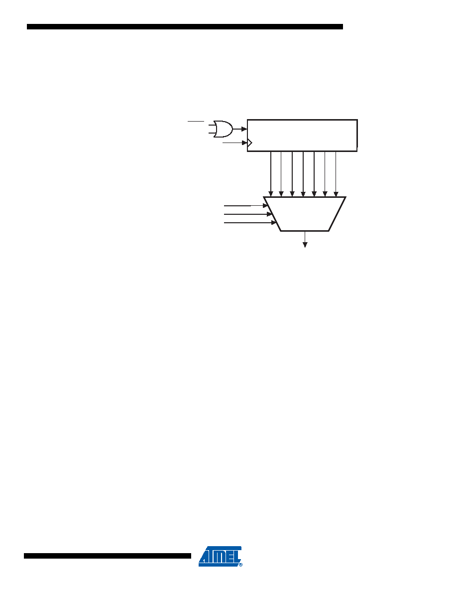
Figure 22-3. ADC Prescaler
By default, the successive approximation circuitry requires an input clock frequency between 50
kHz and 200 kHz to get maximum resolution. If a lower resolution than 10 bits is needed, the
input clock frequency to the ADC can be higher than 200 kHz to get a higher sample rate.
The ADC module contains a prescaler, which generates an acceptable ADC clock frequency
from any CPU frequency above 100 kHz. The prescaling is set by the ADPS bits in ADCSRA.
The prescaler starts counting from the moment the ADC is switched on by setting the ADEN bit
in ADCSRA. The prescaler keeps running for as long as the ADEN bit is set, and is continuously
reset when ADEN is low.
When initiating a single ended conversion by setting the ADSC bit in ADCSRA, the conversion
starts at the following rising edge of the ADC clock cycle.
A normal conversion takes 13 ADC clock cycles. The first conversion after the ADC is switched
on (ADEN in ADCSRA is set) takes 25 ADC clock cycles in order to initialize the analog circuitry.
The actual sample-and-hold takes place 1.5 ADC clock cycles after the start of a normal conver-
sion and 13.5 ADC clock cycles after the start of an first conversion. When a conversion is
complete, the result is written to the ADC Data Registers, and ADIF is set. In Single Conversion
mode, ADSC is cleared simultaneously. The software may then set ADSC again, and a new
conversion will be initiated on the first rising ADC clock edge.
When Auto Triggering is used, the prescaler is reset when the trigger event occurs. This assures
a fixed delay from the trigger event to the start of conversion. In this mode, the sample-and-hold
takes place two ADC clock cycles after the rising edge on the trigger source signal. Three addi-
tional CPU clock cycles are used for synchronization logic. When using Differential mode, along
with Auto triggering from a source other than the ADC Conversion Complete, each conversion
will require 25 ADC clocks. This is because the ADC must be disabled and re-enabled after
every conversion.
7-BIT ADC PRESCALER
ADC CLOCK SOURCE
CK
ADPS0
ADPS1
ADPS2
CK/128
CK/2
CK/4
CK/8
CK/16
CK/32
CK/64
Reset
ADEN
START
发布紧急采购,3分钟左右您将得到回复。
相关PDF资料
PIC16C716-20I/P
IC MCU OTP 2KX14 A/D PWM 18DIP
PIC18F26K80-I/SO
MCU PIC 64KB FLASH 28SOIC
PIC18F26J13-I/SS
IC PIC MCU 64KB FLASH 28SSOP
SFW27R-1STE1
SFW27R-1STE1-FFC/FPC CONN
PIC18F66J15-I/PT
IC PIC MCU FLASH 48KX16 64TQFP
PIC24FV32KA302-I/SO
MCU 32KB FLASH 2KB RAM 28-SOIC
PIC24HJ64GP204-I/ML
IC PIC MCU FLASH 64K 44-QFN
SFW27R-2STE1
SFW27R-2STE1-FFC/FPC CONN
相关代理商/技术参数
PIC16F916-I/SO
功能描述:8位微控制器 -MCU 14KB FL 352R 25 I/O RoHS:否 制造商:Silicon Labs 核心:8051 处理器系列:C8051F39x 数据总线宽度:8 bit 最大时钟频率:50 MHz 程序存储器大小:16 KB 数据 RAM 大小:1 KB 片上 ADC:Yes 工作电源电压:1.8 V to 3.6 V 工作温度范围:- 40 C to + 105 C 封装 / 箱体:QFN-20 安装风格:SMD/SMT
PIC16F916-I/SO
制造商:Microchip Technology Inc 功能描述:8 Bit Microcontroller Clock Speed:20MHz
PIC16F916-I/SOG
制造商:Microchip Technology Inc 功能描述:8BIT MCU FLASH SMD 16F916 SOIC28
PIC16F916-I/SP
功能描述:8位微控制器 -MCU 14KB FL 352R 25 I/O RoHS:否 制造商:Silicon Labs 核心:8051 处理器系列:C8051F39x 数据总线宽度:8 bit 最大时钟频率:50 MHz 程序存储器大小:16 KB 数据 RAM 大小:1 KB 片上 ADC:Yes 工作电源电压:1.8 V to 3.6 V 工作温度范围:- 40 C to + 105 C 封装 / 箱体:QFN-20 安装风格:SMD/SMT
PIC16F916-I/SP
制造商:Microchip Technology Inc 功能描述:8 Bit Microcontroller Clock Speed:20MHz
PIC16F916-I/SS
功能描述:8位微控制器 -MCU 14KB FL 352R 25 I/O RoHS:否 制造商:Silicon Labs 核心:8051 处理器系列:C8051F39x 数据总线宽度:8 bit 最大时钟频率:50 MHz 程序存储器大小:16 KB 数据 RAM 大小:1 KB 片上 ADC:Yes 工作电源电压:1.8 V to 3.6 V 工作温度范围:- 40 C to + 105 C 封装 / 箱体:QFN-20 安装风格:SMD/SMT
PIC16F916-I/SS
制造商:Microchip Technology Inc 功能描述:8-Bit Microcontroller IC
PIC16F916T-E/MLC02
制造商:Microchip Technology Inc 功能描述: